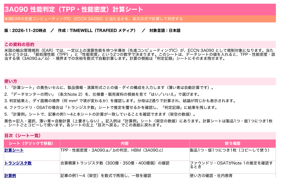
ECCN 3A090 Performance (TPP and Performance Density) Calculator (editable Excel)
Enter datasheet values to calculate TPP, performance density and the applicable 3A090 paragraph using the EAR formulas, with worked examples and a decision record (Japanese only).
Get the fileYou can download it after a short form (Japanese).
Hello, this is Ryuta Hamamoto from TIMEWELL.
Take an export control officer at a semiconductor maker who has just been asked to classify a new product before volume production. Sales says, "It's not for data centers. It's a consumer inference chip." All that has come from the design team is a datasheet and a photo of the die. Does the chip fall under ECCN 3A090, the entry for advanced computing integrated circuits (ICs) in the U.S. Export Administration Regulations (EAR)? If it does, is it 3A090.a or 3A090.b?
The text sets its performance thresholds in numbers. What trips people up in practice is how to arrive at those numbers. Can you take the TOPS figure off the datasheet as it is? How much of the die area counts? How do you add things up for chiplets? And since the new rule from the U.S. Bureau of Industry and Security (BIS) on 19 November 2026, the treatment of foundries has changed too.
This article is a practical guide to classifying under 3A090 from the definitions in the text, all the way from the calculation to the record. Which destinations need a U.S. license, and the controls on remote access to data centers, are left to other articles. Here we focus on one question: which paragraph of 3A090, if any, an IC falls under.
The conclusion first
- Classification under 3A090 turns on two numbers: the highest TPP, and the performance density derived from the area of the non-planar logic dies.
- The rule of 19 November 2026 did not change these thresholds or formulas. What changed is how foundries can overcome the presumption.
- Keep the basis for the calculation in your classification record, down to the datasheet version and the area figures.
What the rule of 19 November 2026 changed for 3A090
First, separate what changed from what did not. The most common mistake in practice is assuming that "a new rule is out, so the thresholds must have changed too."
We compared the 3A090 text published in the Federal Register (91 FR 74970, 19 November 2026) with the text of the same ECCN in the eCFR before the rule took effect (as of 17 November 2026)12. The numerical conditions in 3A090.a, b and c, and the wording of the Technical Notes on TPP and performance density, matched apart from differences in symbols and spacing and one word in the eCFR (in Technical Note 2, paragraph 2, the eCFR reads "annual" where the Federal Register reads "manual"). Nothing in the preamble explains any change to the thresholds or formulas either.
Four things did change.
| Change | What | Effect on classification |
|---|---|---|
| License requirements table | The worldwide license requirement that applied to 3A090.a (former §742.6(a)(6)(iii)(A)) was removed. The whole entry except 3A090.c is now covered by two rows: "the five countries in §742.6(a)(6)(iii)(A)(1)" and "the United Arab Emirates and D:1, D:4 and D:5 (excluding any destination also in A:5 or A:6)" | Classification by paragraph (a or b) is unchanged. Whether a license is needed is a question for other provisions |
| License exceptions | AIA (§740.27) and LPP (§740.29) were removed. ACM and NAC/ACA remain | Rebuild any classification flow that assumed those exceptions |
| Note 1, paragraphs b and c | If the designer is located in D:1, D:4, D:5 or the five countries, or has an ultimate parent headquartered there, a transistor-count attestation cannot overcome the presumption | Practice changes for foundries and OSATs |
| New §744.23(a)(3)(i)(C) | A license requirement when a foundry or OSAT exports, reexports or transfers a 3A090.a IC from a designer that is neither approved nor authorized | Foundries and OSATs have to check whether a license is needed, whatever the destination |
The changes concerning foundries (the EAR's "front-end fabricators") and OSATs (outsourced semiconductor assembly and test companies) are covered in detail in our article on the reported TSMC and Samsung China shipment pause. This article deals with the calculation that leads into the "presumption" discussed there: how to work out transistor counts and TPP.
The U.S. foreign direct product rule (FDPR) and de minimis belong to another article. In brief, section IV.D of the preamble says BIS has not changed §734.9(h). It does, however, restate how broadly that provision applies. For a foreign-produced item that is subject to the EAR under §734.9(h), if a 3A090 IC is incorporated into a foreign-produced part, component, computer or equipment (such as a GPU board or server), BIS continues to have jurisdiction over the IC, and license requirements may apply to the IC and, by extension, the server1. For more, see our article on the reach of the FDPR.
The classification flow: seven questions
Classification works through the following seven questions in order. If your record follows the same order, it is easier to review later.
| Question | What to check | Basis |
|---|---|---|
| 1. Type of item | An IC with digital processing units (a, b), or high bandwidth memory (HBM, c) | The text of 3A090 |
| 2. Subject to the EAR? | Whether the IC is subject to the EAR | Other articles: FDPR, de minimis, U.S. origin and so on |
| 3. TPP | The highest TPP for the whole chip | Technical Note 2 |
| 4. Performance density | TPP ÷ applicable die area | Technical Note 2, paragraph 4 |
| 5. Applying the thresholds | Which of a.1, a.2, b.1 and b.2 applies, if any | 3A090.a and b |
| 6. The data center question | Whether it is designed or marketed for use in datacenters | Note 2, NAC/ACA |
| 7. Extra checks by role | For foundries and OSATs, the Note 1 presumption. For products that incorporate the IC, the knock-on effect on .z paragraphs and 4A090 | Note 1, Note 4 |
Why question 6 comes after question 5
There is a trap in the order of reading. Note 2 says that 3A090.a and 3A090.b "do not apply to items that are not designed or marketed for use in datacenters and do not have a 'total processing performance' of 4800 or more"1. So even if the numbers reach a threshold, an item with a TPP below 4800 that is not for data centers falls outside 3A090.a and b.
Reading the provisions together takes us one step further. 3A090.a.1 catches any item with a TPP of 4800 or more, whatever its performance density. That leaves 3A090.b with items whose TPP is below 4800. Because of Note 2, 3A090.b can therefore be read as limited to items designed or marketed for use in datacenters. This is our reading of the text. We have not confirmed whether BIS explains it the same way.
An item with a TPP of 4800 or more that is not for data centers is 3A090.a. In that case, the ECCN entry says it may be eligible for License Exceptions NAC and ACA1.
We could not find a definition of "designed or marketed for use in datacenters" in the parts of the EAR we checked (Parts 740, 744 and 772)2. So you need to record the design specifications, sales materials, customers' uses and the form of the product (card, server, embedded module) as the basis for your decision. Calling the chip "consumer" internally is not a basis.
Different roles answer different questions
Even for the same 3A090, which questions a company has to answer depends on its role.
| Role | Main questions | What to watch |
|---|---|---|
| Designer (fabless, IDM) | 3, 4, 5, 6 | Works out the performance figures from its own data. These figures are the source of any attestation given to the foundry |
| Foundry or OSAT | 7 (the Note 1 presumption), 5, 6 | Only these two face the presumption. Either receive the designer's attestation or do the calculation yourself |
| Distributor or trading company | Checking the classification received | When you receive a designer's classification, check the version and date |
| Board or server maker | Classification of the incorporated IC, knock-on effect on .z paragraphs and 4A090 | The IC's classification determines the product's |
Note 1 states that the presumption "does not apply to any entity other than the 'front-end fabricator' or 'OSAT' company"1. Designers and distributors do not need to apply it to themselves. They classify from the actual specifications.
Replace siloed classification work with AI.
METI's FY2024 data shows 52% of foreign exchange law violations stem from classification errors. Download the TRAFEED product catalog covering features and rollout.
Turning the text into numbers you can calculate
From here, each definition is turned into something you can calculate. The wording of the text is as in the Federal Register. Our own explanations are in the "In plain terms" column.
| Term | Definition in the text (summary) | In plain terms | Watch out |
|---|---|---|---|
| Total processing performance (TPP) | 2 × MacTOPS × bit length of the operation, aggregated over all processing units on the IC | Operations per second multiplied by the bit width of each operation | Where there are several bit lengths, use the highest TPP |
| MacTOPS | The theoretical peak number of tera (10¹²) operations per second for multiply-accumulate computation (D = A × B + C) | Compute performance counting a multiply-accumulate as one operation. Doubled, it is close to TOPS or FLOPS | "Theoretical peak." Use the highest value in the manufacturer's materials |
| Bit length of the operation | The largest bit length of the inputs to the multiply operation in a multiply-accumulate computation | How many bits go into the multiplication | The text sets it by the width of the inputs |
| Dense and sparse | For ICs that process both sparse and dense matrices, the value for dense matrices (without sparsity) | Leave out the speed-up from sparsity | Datasheets tend to headline sparse figures |
| Applicable die area | Measured in millimeters squared; includes all die area of logic dies manufactured with a process node that uses a non-planar transistor architecture | The area of the leading-edge compute dies | How planar dies and memory are treated is discussed below |
| Performance density | TPP ÷ applicable die area | Compute per unit of area | Higher for small, powerful chips |
| Approximated transistor count | The die's transistor density (the number of transistors that can be fabricated per mm² at the process node) × die area (mm²) | A figure near the upper limit, from the node's theoretical density | Comes out higher than the real count. If it is low, you are on the safe side |
| Aggregated approximated transistor count | The sum of the approximated transistor counts of the logic dies in the final package fabricated at the 16/14 nm node or below, or with a non-planar transistor architecture (§772.1) | The leading-edge logic dies in the package, added together | Planar dies at older nodes are not counted. A planar die at 16/14 nm or below is |
Technical Note 2, paragraph 1 sets out the TPP formula: "'Total processing performance' ('TPP') is 2 × 'MacTOPS' × 'bit length of the operation', aggregated over all processing units on the integrated circuit." Paragraph 1.b adds: "The 2 in the 'TPP' formula is based on industry convention of counting one multiply-accumulate computation, D = A × B + C, as 2 operations for purpose of datasheets. Therefore, 2 × MacTOPS may correspond to the reported TOPS or FLOPS on a datasheet."1
Which TPP figure to use
Technical Note 2, paragraph 2 says the rate of MacTOPS "is to be calculated at its maximum value theoretically possible" and "is assumed to be the highest value the manufacturer claims in a manual or brochure for the integrated circuit"1. By way of example, it says the TPP threshold of 4800 "can be met with 600 tera integer operations (or 2 × 300 'MacTOPS') at 8 bits or 300 tera FLOPS (or 2 × 150 'MacTOPS') at 16 bits."
That example gives a practical shortcut. If the datasheet's TOPS or FLOPS counts a multiply-accumulate as two operations, TPP comes out at roughly "datasheet figure × bit length." But the text only says "may correspond." Check with the designer how the datasheet counts.
For an IC that can multiply-accumulate at several bit lengths, calculate the TPP for each and use the highest1. If it can do both 8-bit integer and 16-bit floating point, calculate both.
What goes into the denominator of performance density
Technical Note 2, paragraph 4 sets the denominator. "Applicable die area" is "measured in millimeters squared and includes all die area of logic dies manufactured with a process node that uses a non-planar transistor architecture"1.
One thing can be said for certain from this: all the area of non-planar logic dies goes into the denominator. If a chiplet design has two compute dies, add the two areas together.
Two things cannot be settled from the text. One is whether the area of an I/O die made on a planar process goes into the denominator. The verb "includes" widens the scope; the text does not say that anything is left out. The other is how memory dies such as HBM are treated. The one sentence in the text does not tell you how anything other than logic dies is handled. BIS's FAQs of December 29, 2023 (on the October 2023 rules), however, answer both: for chiplets, count only the area of each logic chiplet in the package that uses a non-planar architecture and exclude chiplets with a planar transistor architecture (II.A1.b), and exclude all HBM area because HBM is memory, not logic (II.A1.c).3 We have not checked whether later amendments changed these answers.
So in practice the safe course is to calculate the denominator both ways. If the conclusion is the same either way, record that and stop there. If it changes, check the designer's basis for the calculation and, if needed, take it to a specialist or put an inquiry to BIS.
Two ways to work out the approximated transistor count
Technical Note 1 to 3A090.a sets out two ways for a foundry or OSAT to work out a die's approximated transistor count1.
The first is to multiply the transistor density of the process node by the die area. The text says this number "may be significantly higher than the true transistor count, but if the result is below the relevant transistor threshold, then the 'front end fabricator' or 'OSAT' company can be confident that the die in question will not exceed that threshold." It is the conservative calculation.
The second, "to adjudicate edge cases," is to "use standard design verification tools to estimate the number of (both active and passive) transistors on the die using the GDS file."
Working through fictitious examples
The examples below walk through the calculation step by step. Every figure in this section is fictitious. None is the specification of a real product. The numbers are there to make the steps visible.
Example 1: a single die for data centers (TPP and performance density)
Datasheet figures for fictitious Chip A (dense, without sparsity):
| Format | Datasheet figure | MacTOPS | Bit length | TPP |
|---|---|---|---|---|
| INT8 | 440 TOPS | 220 | 8 | 2 × 220 × 8 = 3,520 |
| FP8 | 440 TFLOPS | 220 | 8 | 3,520 |
| FP16 | 220 TFLOPS | 110 | 16 | 2 × 110 × 16 = 3,520 |
| FP32 (vector) | 60 TFLOPS | 30 | 32 | 2 × 30 × 32 = 1,920 |
| INT8 (sparse) | 880 TOPS | Not used | Not used | Not used (dense values only) |
The highest TPP is 3,520, so that is the figure to use. The chip has one non-planar logic die, with an area of 600 mm².
- Performance density = 3,520 ÷ 600 = 5.867
- TPP is below 4800, so a.1 does not apply
- a.2 requires a TPP of 1600 or more and a performance density of 5.92 or more. 5.87 is below 5.92, so a.2 does not apply
- b.1 requires a TPP of 2400 or more and less than 4800, and a performance density of 1.6 or more and less than 5.92. b.1 applies
The conclusion: 3A090.b, if the chip is for data centers. But these figures were picked on purpose to sit near a boundary. The die area at which performance density reaches 5.92 is 3,520 ÷ 5.92 ≈ 594.59 mm². With a die area of 594 mm², performance density is 5.926 and the chip is 3A090.a.2. At 595 mm² it is 5.916, and the chip is 3A090.b. One square millimeter changes the paragraph. That is why you confirm with the designer, and record, how the area was measured (whether the scribe line is included, and whether it is a design dimension or a measured value). You can rerun this example, and find the area at which the paragraph flips, in our 3A090 TPP and performance density calculator (Excel, in Japanese). You enter datasheet values and it applies the formulas in the text to give TPP, performance density and the paragraph, with worked examples and a record sheet.
Example 2: a chiplet design (calculating the denominator both ways)
Fictitious Chip B has two non-planar logic dies (300 mm² each) and one I/O die made on a planar process (100 mm²). TPP for the whole package is 3,520.
| Denominator | Area | Performance density | Paragraph |
|---|---|---|---|
| Non-planar logic dies only | 600 mm² | 5.87 | 3A090.b (if for data centers) |
| Including the I/O die | 700 mm² | 5.03 | 3A090.b (if for data centers) |
Either way, the conclusion is 3A090.b. In the record, write something like: "The text does not settle how the planar I/O die is treated, so we calculated both ways. The conclusion is the same." If the figures would change the conclusion, stop here and check the designer's basis for the calculation.
Example 3: a foundry works out the approximated transistor count
Suppose a foundry packages fictitious Chip B, with its two non-planar logic dies (300 mm² each) and one planar I/O die. The example is there to show the structure of the text. Assume the conditions on the designer's location and so on are met (if they are not, this calculation cannot overcome the presumption).
Start with what counts. A planar I/O die at an older node is not within the definition of the aggregated approximated transistor count. The definition covers logic dies at the 16/14 nm node or below, or with a non-planar architecture, so a planar die at 16/14 nm or below is covered2. With the first method, take a fictitious density of 120 million transistors per square millimeter: 120 million × (300 + 300) = 72 billion. That is far above the 30 billion threshold, though the figure may be higher than the true count. With the second method, suppose the estimate from the GDS file comes to a fictitious 38 billion. That is still above the 30 billion threshold.
The thresholds in the text are 30 billion, 35 billion and 40 billion transistors. (In Japanese these are written 300億, 350億 and 400億. If you work with Japanese documents or colleagues, watch out for 30 billion being misread as 30億, which is only 3 billion.) Applied to 38 billion:
| Package condition | Thresholds available | Result for 38 billion |
|---|---|---|
| Contains HBM | 30 billion only | Above. Cannot overcome the presumption |
| No HBM; export, reexport or transfer completed in 2027 | 30 billion or 35 billion | Above. Cannot overcome the presumption |
| No HBM; export, reexport or transfer completed in 2029 or later | 30 billion or 40 billion | Below 40 billion. Can overcome the presumption if the other conditions are met |
If the estimate were instead, say, a fictitious 33 billion, with no HBM and an export in 2027, it would fall below the 35 billion threshold (it is above 30 billion, so the 35 billion allowance is needed). With HBM, it would be above 30 billion and could not overcome the presumption. The text can be read as saying that only where these conditions line up, and the conditions on the designer's location and so on are also met, can the foundry overcome the presumption by attestation1. The 2029 allowance lies beyond the date of this article. Check the text as it stands at that time.
Example 4: classifying HBM (3A090.c)
3A090.c covers "high bandwidth memory (HBM) having a 'memory bandwidth density' greater than 2 gigabytes per second per square millimeter"1. Memory bandwidth density is the memory bandwidth in gigabytes per second divided by the area of the package or stack in square millimeters. Where a stack is contained in a package, use the memory bandwidth of the packaged device and the area of the package.
In a fictitious example, if the package's memory bandwidth is 1,000 GB/s and the package area is 120 mm², then 1,000 ÷ 120 = 8.3, which is above 2. The item falls under 3A090.c.
The Technical Note draws two boundaries. DRAM ICs are included if they exceed this density, even if they do not conform to the JEDEC standards for HBM. On the other hand, co-packaged products containing both HBM and a logic IC, where the dominant function is processing, are outside the control. HBM permanently affixed to a logic IC designed as a control interface and incorporating a physical layer (PHY) function is, however, included1.
Questions to put to the designer or foundry
As the four examples show, the calculation needs information that is not on the datasheet. The table below lists what to confirm in writing with the designer (or the foundry).
| Item to confirm | Why | Form of answer |
|---|---|---|
| Product name, model number and SKU; datasheet version and date | To show later which version the classification was based on | In writing |
| Dense peak values (TOPS, FLOPS) for each format | TPP calculation | The relevant datasheet page |
| Whether those TOPS and FLOPS figures count a multiply-accumulate as two operations | Matching the "2" in the TPP formula | Explanation from the designer |
| Bit width of the inputs to the multiplier (especially for formats such as TF32, whose name and width differ) | Bit length of the operation | Explanation from the designer |
| Number of processing units and how they are aggregated | Total across all processing units | Explanation from the designer |
| Die configuration (number of dies, process node of each, planar or non-planar, area) | Performance density and transistor count | A table |
| How area is measured (design dimension or measured; treatment of the scribe line) | Decisions near a boundary | Explanation from the designer |
| Whether HBM is included, and how many stacks | Choice of transistor-count threshold; 3A090.c | A table |
| Location of the designer and of its ultimate parent's headquarters | Conditions in Note 1, paragraphs b and c | In writing |
| Whether the designer is an approved IC designer (Supplement No. 6) or an authorized IC designer | Note 1, paragraph a | In writing |
| Whether the product is designed or sold for data centers | Note 2 | Specifications, sales materials |
| Form of the product (card, server, embedded) | Recording how it is actually sold | Product materials |
| Where it is packaged, and the OSAT's name | Note 1, paragraphs b and c (whether it is an approved OSAT) | In writing |
The template below can be used for an inquiry to the designer. It is only a template. Do not send it as it is; have it reviewed by your legal team or a specialist first.
Template (inquiry to the designer under the EAR; written for Japanese business practice, to be reviewed by your legal team or a specialist)
Regarding [product name] (model number [X], datasheet version [X], dated [date]), please answer the following in writing so that we can classify the product under ECCN 3A090 of the U.S. Export Administration Regulations (EAR).
- For each format (INT8, FP8, FP16 and so on), the peak value without sparsity, and whether that value counts a multiply-accumulate as two operations.
- For each format, the bit width of the inputs to the multiplier.
- The die configuration. For each die: the process node, the transistor architecture (planar or non-planar) and the area (including how it is measured).
- Whether HBM is included, and how many stacks.
- The location of your company and of your ultimate parent company's headquarters.
- Whether this product is designed or sold for data centers, and the materials that support your answer. We will keep your answers as part of our classification record.
Where a classified item stands, and how to keep the record
Once you have a result, check the following three things. Whether a license is actually needed depends on the provisions on destinations and parties, so this article does not go into it in detail.
Where the license exceptions stand
The license exceptions paragraph of ECCN 3A090 reads as follows1.
| Exception | What the 3A090 entry says | Where it stands in practice |
|---|---|---|
| NAC/ACA | Yes for 3A090.a if the item is not designed or marketed for use in datacenters and has a TPP of 4800 or more. Yes for 3A090.b if the item is designed or marketed for use in datacenters. N/A for 3A090.c | §740.8. NAC is a notification, ACA an authorization. Conditions apply, such as a written purchase order2 |
| ACM | Yes | §740.28. For "development," "production" or storage by private sector end users, for items ultimately destined to customers outside Macau and D:5. Not available where the ultimate consignee, or its ultimate parent, is headquartered in Macau or D:5. For 3A090.a, only items designed by an approved or authorized IC designer2 |
| HBM | Yes for 3A090.c (§740.25) | For 3A090.c |
| AIA, LPP | Removed by the rule of 19 November 2026 | Take them out of old classification flows |
The preamble explains that ACM was kept "due to the benefits this license exception plays in supporting the supply chains of export, reexports, and transfers (in-country) of advanced SI items destined to ultimate end users outside of Macau or destinations in Country Group D:5"1. Note, though, that §740.2(a)(9)(ii) limits which license exceptions can be used for 3A090 and similar items to certain destinations. Check that provision as well before relying on an exception.
What the report needs
The new §743.10 requires monthly reports as the condition for excluding customers headquartered in the U.S. (or whose ultimate parent is) from the license requirement for five countries (Indonesia, Malaysia, Singapore, Brazil and Thailand). Reports are due monthly, by the first business day of the month after the transaction. The required information includes the ECCN with the paragraph-level classification (for example, 3A090.a), the product name and SKU, the product's TPP and the quantity, along with each party's name, address and phone number, the ultimate parent, the destination and the date of export, reexport or transfer1.
In other words, the classification record doubles as material for the report. If you pin the classification down to the paragraph and keep TPP as a figure, you will not need to redo the calculation for every report.
Example classification record
Records under the EAR must, as a rule, be kept for five years from the latest of the relevant times, such as the export or the termination of the transaction (§762.6)2. We recommend one record in the format below for each product and each version. It is an example only; adapt it to your own forms.
| Field | Example entry (fictitious) |
|---|---|
| Product name, model number, SKU | Fictitious Chip A, model AX-100 |
| Date of classification, classifier, approver | 2026-11-20, export control staff [name], officer [name] |
| Source documents and versions | Datasheet v1.3 (dated 2026-10-15), designer's written answers (dated 2026-11-18) |
| TPP calculation | INT8 440 TOPS (dense), MacTOPS 220, 2 × 220 × 8 = 3,520. Highest value 3,520 |
| Applicable die area | One non-planar logic die, 600 mm² (design dimension, per the designer's answers) |
| Performance density | 3,520 ÷ 600 = 5.867 |
| Applying the thresholds | a.1: no; a.2: no (5.867 is below 5.92); b.1: yes |
| Sensitivity to area (near a boundary) | Becomes 3A090.a.2 at about 594.59 mm² or less. Designer asked to confirm the area |
| Data center question (Note 2) | Designed for data centers per the design specification; sold the same way |
| Result | 3A090.b |
| HBM (3A090.c) | Whether HBM is built in, and its memory bandwidth density |
| License exceptions under consideration | NAC/ACA, ACM. Note where the conditions were checked |
| Rule relied on | The text of 91 FR 74970 (effective 19 November 2026) |
| Triggers for reclassification | A new datasheet version, a change in die area, an amendment of the rule |
The template below is one way to record the result internally. It is a template, to be used on the understanding that it will be reviewed.
Template (internal classification note; to be reviewed by your legal team or a specialist)
Product AX-100 (datasheet v1.3) has a highest TPP of 3,520 on dense values, an applicable die area of 600 mm² (per the designer's written answers) and a performance density of 5.867. It does not meet the conditions of ECCN 3A090.a.1 (TPP of 4800 or more) or a.2 (performance density of 5.92 or more), and it meets the conditions of b.1 (TPP of 2400 or more and less than 4800, performance density of 1.6 or more and less than 5.92). Because it is designed and sold for data centers, it is not excluded under Note 2, and it is classified as 3A090.b. If the die area is about 594.59 mm² or less, it becomes 3A090.a.2. We have asked the designer to confirm in writing how the area is measured.
Common mistakes, and what to look at when reviewing
When you review a classification record, where should you look first? Here are the mistakes that tend to happen in practice, set against the text.
The first is units. Mixing up TOPS and MacTOPS, or how FLOPS figures count multiply-accumulates, doubles or halves TPP. The text explains the "2" in the formula as matching the way datasheets count, so confirm the counting with the designer. The second is using sparse figures. The headline number on a datasheet is often the figure with sparsity, and Technical Note 2, paragraph 3 says to use the dense values1.
The third and fourth are about which value you pick. Where TPP differs between bit lengths, such as 8-bit and 16-bit, use the highest TPP, not a typical one. That holds even for formats you would not choose for the intended use or in normal operation. And Technical Note 2, paragraph 2 says to use "the highest value the manufacturer claims in a manual or brochure," so benchmark results are not the yardstick.
The fifth is counting dies. Do not use the area of the whole package in place of the chiplets' area, and do not mix HBM area into logic die area. Add up every non-planar logic die, without missing any.
The sixth and seventh happen at the judgment stage. Settling the data center question on the sales team's word is the sixth. Note 2 asks how the item is actually "designed" or "marketed," and the basis is the wording in specifications and sales materials, not what the item is called internally. The seventh is applying the foundry and OSAT presumption to designers or distributors. Note 1 limits the presumption to foundries and OSATs. Conversely, paragraph d of Note 1 does not let foundries or OSATs settle the matter on an end user's attestation alone1.
The last three concern years, versions and records. The eighth is getting the years wrong for the transistor-count thresholds. Sub-paragraph (b) of paragraphs b and c sets 35 billion for "exports, reexports, or transfers (in-country) completed in 2027" and 40 billion for those "completed in 2029 or thereafter." The text does not give the 35 billion or 40 billion allowance for packages without HBM for 2026 or for 2028. Whether only the 30 billion threshold is available in those two years, or something else applies, cannot be confirmed from the text, so check the text itself. The ninth is classifying on an old version of the text: make sure no classification flow that relies on removed exceptions such as AIA and LPP is still in use internally. The tenth is recording only the conclusion. A record that holds only the conclusion cannot be reviewed when the rule or the datasheet changes. Keep the calculation and the versions of the documents.
What we have not confirmed, and the limits of this article
To finish, here is what we have not been able to confirm, and what this article leaves out.
First, the version of the text. We checked the 3A090 text in the published Federal Register (91 FR 74970). We compared it with the eCFR before the rule took effect (as of 17 November 2026) and confirmed that the numerical conditions and the wording of the Technical Notes match. In the eCFR, the phrase in Technical Note 2, paragraph 2 about "the highest value the manufacturer claims" read "annual or brochure," while the published Federal Register reads "manual or brochure." We treat the Federal Register as authoritative12.
The one sentence in the text does not settle whether planar I/O dies or memory dies go into the denominator of performance density. BIS's FAQs of December 29, 2023 say to exclude planar chiplets and HBM area, but they concern the October 2023 rules, and we have not checked whether later amendments changed those answers. We did not check other BIS guidance or advisory opinions for this article. Nor did we find a definition of "for data centers" in the parts of the EAR we checked.
How to read paragraph d of Note 1 is still open, too. As a matter of sentence structure, this paragraph of the Federal Register text is hard to follow. The intent of the presumption where the foundry cannot confirm the transistor count comes through, but check the details in the original. How the wording of paragraph d relates to the preamble of the January 2025 rule that created the presumption is set out, with the original text, in our article on the foundry provisions. The years for the transistor-count thresholds are similar: the text does not give the 35 billion or 40 billion allowance without HBM for 2026 or 2028, and we have not confirmed how those years are treated.
Japan's system is outside the scope of this article. Classification under Japan's Foreign Exchange and Foreign Trade Act (FEFTA) is not covered, and classifying under 3A090 of the EAR does not replace classification under Japan's Goods Ordinance, issued by the Ministry of Economy, Trade and Industry (METI). For the Japanese side, see our explainer on METI's Q&A for computers, electronics, ICs and semiconductor materials (in Japanese) and our article on export control for semiconductor equipment makers. What happens next to the rule is also open. The rule of 19 November 2026 is an interim final rule, and the comment period runs until 19 January 2027. Its content may change1.
This article is a general summary of information. For decisions on specific products or transactions, consult your internal export control officer and specialists (and, where needed, BIS or METI). We do not intend to evaluate any specific company mentioned in this article. One square millimeter can change the paragraph, so if you are unsure, start by writing down the basis for your numbers.
What to read next
- Reported TSMC and Samsung China shipment pause: what the new BIS foundry rule changed
- GPU cloud and export controls: sorting facts on the new BIS rule and reports on a Japanese company
- Foreign Direct Product Rule (FDPR) explained: de minimis differences and what Japanese firms miss
- BIS advanced computing guidance (31 May 2026)
- U.S.-China AI semiconductor regulation calendar 2024-2026
- Semiconductors and economic security: a map from industry structure to export controls
- Reports of Nvidia chip purchases by Chinese universities: what to check before you trade with one
- Customer due diligence (end-user screening) in practice
If you are struggling to set up a way for your team to run classification records and counterparty checks, talk to us through the TRAFEED inquiry form.
Footnotes
-
U.S. Department of Commerce, Bureau of Industry and Security (BIS), "Addressing Remote Access to Advanced Semiconductors," interim final rule, Federal Register, 91 FR 74970 (19 November 2026; FR Doc. 2026-23529; RIN 0694-AK50). We checked the following in the published Federal Register text on 20 November 2026: the text of ECCN 3A090 (a, b and c, Notes 1 to 4, Technical Notes 1 and 2), §742.6(a)(6)(iii), §743.10, §744.23(a)(3)(i), the §772.1 definition of "Aggregate TPP," preamble sections IV.D (foreign direct product rules), IV.E (ACM) and V (changes to Note 1), and the savings clause. https://www.federalregister.gov/documents/2026/11/19/2026-23529/addressing-remote-access-to-advanced-semiconductors . We obtained the full published text and checked the 3A090 entry and the related provisions. ↩ ↩2 ↩3 ↩4 ↩5 ↩6 ↩7 ↩8 ↩9 ↩10 ↩11 ↩12 ↩13 ↩14 ↩15 ↩16 ↩17 ↩18 ↩19 ↩20
-
Electronic Code of Federal Regulations (eCFR), Title 15, as of 17 November 2026 (before the rule of 19 November 2026 took effect). On 20 November 2026 we checked §772.1 (the definitions of "aggregated approximated transistor count," "applicable advanced logic integrated circuits," "front-end fabricator" and "Outsourced Semiconductor Assembly and Test (OSAT)"), §740.8 (NAC/ACA), §740.28 (ACM), §762.6 (period of retention) and ECCN 3A090 in Part 774 (the text before amendment). https://www.ecfr.gov/ . The rule of 19 November 2026 adds a definition of "Aggregate TPP" to §772.1 and removes the definition of "Model Weights"; we have not identified any change to the other definitions listed above. ↩ ↩2 ↩3 ↩4 ↩5 ↩6 ↩7
-
BIS, "Frequently Asked Questions (FAQs) for 'Export Controls on Semiconductor Manufacturing Items' (SME IFR) and 'Implementation of Additional Export Controls: Certain Advanced Computing Items; Supercomputer and Semiconductor End Use; Updates and Corrections' (AC/S IFR)" (FAQ Date: December 29, 2023), II.A1.b and II.A1.c. https://www.bis.gov/media/documents/2023-frequently-asked-questions-003-clean-posting.pdf . Checked against a copy retrieved on November 22, 2026. ↩